Microchips, despite their tiny size, are incredibly important for the working of nearly all the electronic devices we use daily. These small but mighty components are found in a wide range of items and systems, from simple home appliances to sophisticated computers.
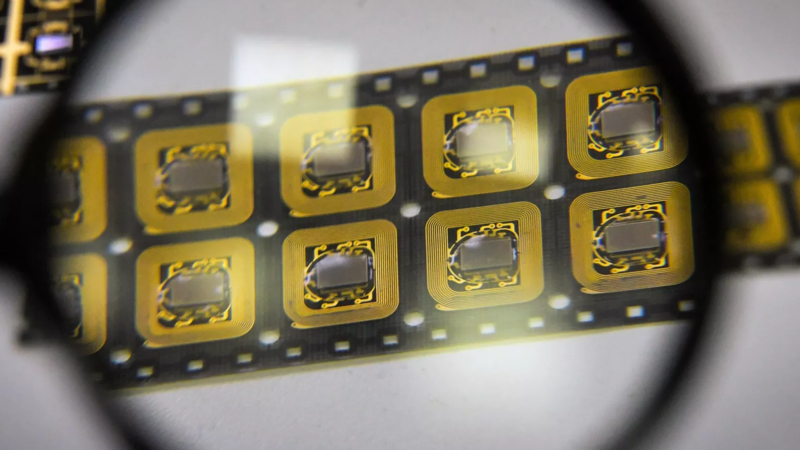
Before we delve into the intricate world of microchips, it’s crucial to answer a basic question: What are the materials used in making microchips? Essentially, microchips are made up of semiconductor materials, with silicon being the primary one, which is key to their operation.
These vital components, at their core, contain semiconductors, which are essential for the functioning of microchips. This discussion aims to delve into the makeup of microchips, highlighting the importance of these materials. By understanding the composition of microchips, we get a glimpse into the technological fabric of our digital age.
For a more in-depth understanding of microchips, it’s worth exploring the evolution of the microchip. This journey traces the fascinating progression from the earliest models to today’s advanced chips, offering valuable insights into the development and influence of this technology.
The Reason Why Semiconductors are Fundamental to Microchips
What exactly are microchips made from? The key lies in semiconductors, the essential elements that make up the core of all microchips. The distinct electrical characteristics of these materials are what empower microchips to carry out their vital roles in a variety of electronic devices.
Semiconductors are the bedrock of microchips, playing a crucial part in how they work. Unlike conductors and insulators, semiconductors are materials that partially conduct electricity, and their electrical properties can be modified through a process called doping (the addition of atoms with positive or negative charges). This unique feature of semiconductors enables them to create active components, like transistors, which are key to managing the flow of electrical current.
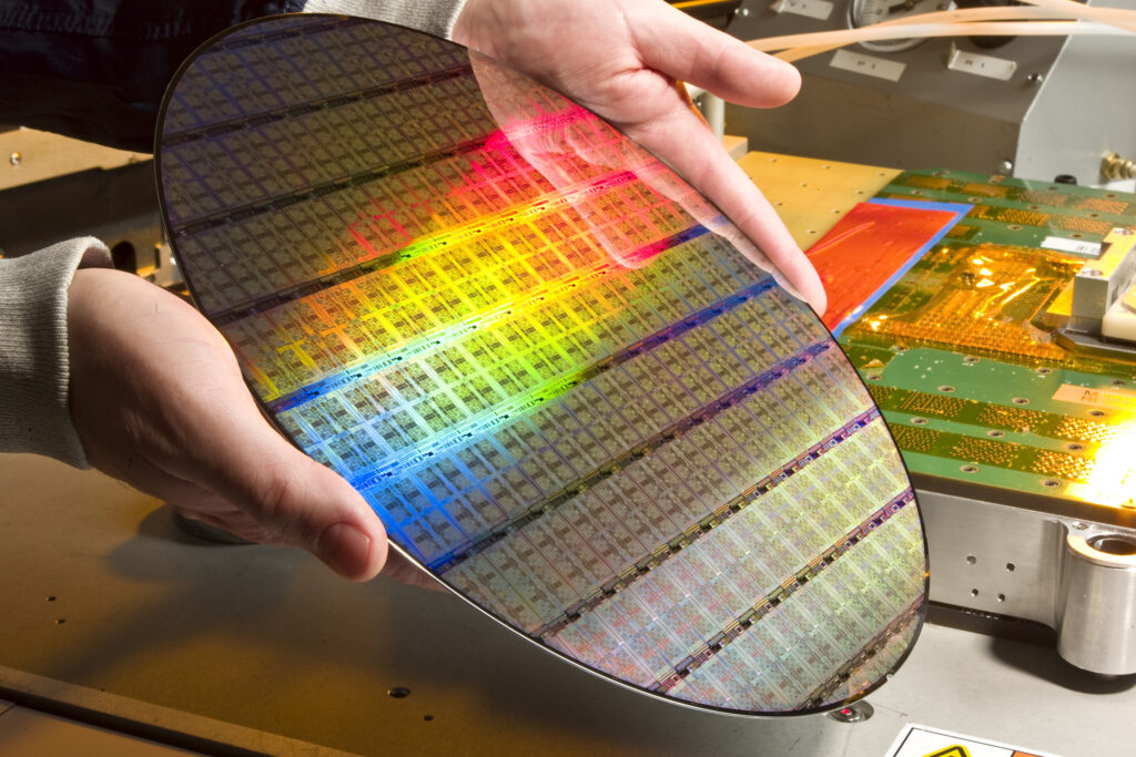
There are many types of semiconductor materials out there, but only a handful have been found to be suitable for use in microchips. This is because of the strict purity and specific electrical property requirements necessary for semiconductors to function effectively. The type of semiconductor material chosen can greatly affect the microchip’s efficiency, speed, and power usage, making this choice a critical part of microchip design.
For those who want to delve deeper into how these complex components are made, our earlier article titled “How do we create Microchips?” provides a detailed overview. It takes you through the intricate process of turning these semiconductor materials into the microchips that drive our digital world. Gaining an understanding of this manufacturing process allows for a greater appreciation of the intricacy and precision needed to create these essential pieces of modern technology.
Rising of Silicon in the Semiconductor Industry
Investigating the rise of silicon in the semiconductor industry helps us understand why this element is the cornerstone of contemporary electronics.
Silicon’s Electrical Excellence When we ask what microchips are made from, the answer invariably leads us to silicon. This material’s perfect balance of conductivity and insulation distinguishes it, making it the go-to choice for microchips. But it’s not just that silicon has ideal electrical properties; it’s also that these properties can be altered more easily than those of other semiconductors. While there are other semiconductors with superior traits, silicon is one of the few that provides an excellent balance between power capabilities, maximum switching speed, and reliability.
Thermal Durability Another major advantage of silicon is its thermal characteristics. Silicon microchips can operate reliably under a range of environmental conditions, enduring both high and low temperatures. This makes them perfect for a wide variety of applications, from automotive electronics, which need to withstand severe temperature changes, to consumer electronics, which typically operate in more controlled environments.
Availability and Accessibility The third factor contributing to silicon’s supremacy is its abundance. Silicon is one of the most abundant elements on Earth, ensuring a consistent and scalable supply, a critical factor for an industry that requires large volumes of raw material. The easy availability of silicon also makes it a cost-effective option for the mass production of microchips, thanks to economies of scale.

Considering the Environment Finally, the environmental consequences of silicon mining are relatively small, particularly when compared to other semiconductor materials. The process of extracting silicon from sand, while energy-consuming, doesn’t result in the same degree of environmental harm or production of toxic byproducts as the mining of some other elements. This factor is becoming increasingly significant in a time when industries worldwide are paying more attention to sustainability and environmental impact.
In conclusion, the prominence of silicon in the semiconductor industry can be attributed to its superior electrical and thermal characteristics, its plentiful supply, and its comparatively minor environmental footprint. These combined factors have established silicon as the preferred material for microchip production, influencing the direction of contemporary electronics.
Investigating Semiconductor Materials Other Than Silicon
While silicon is the reigning champion in the semiconductor industry, it’s not the only player in the game. There are certain applications where other semiconductor materials are not just advantageous, but essential.
When we ask what microchips are composed of, we discover that beyond silicon, materials like Indium Gallium Nitride and Aluminium Gallium Indium Phosphide have a significant role in specific applications, such as the manufacturing of LEDs.
LEDs: A Scenario Where Silicon Doesn’t Shine
A perfect example of an application that requires different semiconductor materials is the production of Light Emitting Diodes (LEDs). The basic principle behind LEDs is that when excited electrons return to lower energy states, they emit light. While silicon is extremely useful in integrated circuits, it’s not suitable for LEDs because the energy levels in silicon can’t produce visible light (it primarily emits infrared photons, which are invisible to the human eye).
Despite their widespread use, the complex workings of LEDs are still a mystery to many. This video unravels the process, diving into the molecular interactions that allow electrons to emit photons and produce light. It also illuminates how scientists and engineers utilize these principles to generate specific colors and package semiconductor material for practical use. Whether you’re an aspiring electronics enthusiast or just interested in the science behind everyday technology, this video provides a thorough and understandable exploration of LED technology.
To create LEDs that emit visible light, various materials are utilized:
- Indium Gallium Nitride (InGaN): This substance is essential for the production of blue and green LEDs, which are vital for a wide range of applications, including display screens and lasers.
- Aluminium Gallium Indium Phosphide (AlGaInP): This substance is employed in the creation of red, yellow, and orange LEDs. Its distinctive characteristics enable efficient light emission in these color ranges, making it a crucial material in the LED industry, from display screens to signal lights.
Germanium: A Flexible Contender Germanium is another semiconductor material worth mentioning. Although it’s not as commonly used as silicon, Germanium has found its unique place, especially in Radio Frequency (RF) applications. Its characteristics make it highly efficient in RF diodes, which are crucial components in a variety of communication and signal processing devices.
Conclusion: The Wide Spectrum of Semiconductors To sum up, while silicon is the most commonly used material for semiconductor applications, the realm of semiconductor materials is diverse and extensive. Materials like Indium Gallium Nitride and Aluminium Gallium Indium Phosphide play vital roles in the LED industry, while Germanium is important in RF applications. These alternative materials underscore the versatility and variety of semiconductor technology, meeting specific requirements that silicon alone cannot address. Gaining an understanding of these alternatives provides a glimpse into the complex and vibrant world of semiconductor applications beyond the realm of silicon.
Silicon Carbide: An Emerging Powerhouse in Semiconductor Substances
Microchips aren’t made from metals like iron or copper. Instead, they’re made from special elements called metalloids. Silicon and silicon carbide are examples of these metalloids.
Even though metalloids aren’t metals, they have some properties that are similar to metals. These metal-like properties are really important for microchips to work the way they do. So, when we talk about what metal microchips are made of, we’re really talking about these metalloid elements and their special properties.

The Rise of Silicon Carbide Silicon Carbide, or SiC for short, is a material that’s getting a lot of attention i
n the world of electronics. It’s a type of semiconductor, which is a material that’s used to make electronic devices. SiC is expected to be really important in the future of electronics because it has some special properties that make it better than the usual silicon, especially for devices that need to be really efficient and powerful.
The process of making these small but mighty parts that power our electronic devices is quite complex. It starts with carefully shaping silicon into thin slices, called wafers. Then, layers of different materials are built up on the wafer. This video takes you through this whole process, showing you all the amazing technology that goes into making microchips. If you’re interested in technology, or just want to know more about how the devices we use every day are made, this video is a great way to learn about the skill and innovation in the semiconductor industry.
Great Heat Handling Silicon Carbide (SiC) is really good at conducting heat. This means that devices made with SiC can work at higher temperatures than those made with silicon. This is useful because it means the devices can be used in more situations, and they’re likely to last longer.
Better Electricity Flow Silicon Carbide can also conduct electricity better than silicon. This means that SiC devices can handle more electrical current for their size, which is important for devices that need a lot of power. Because SiC is more efficient, it also loses less energy, which makes it a good choice for devices where saving energy is important.
Small but Powerful Because of its special properties, Silicon Carbide can be used to make smaller devices than silicon. This is a big advantage, especially for devices where space is limited. Being able to fit more power into a smaller space opens up new possibilities for designing and building electronic devices.
Perfect for Power Amplifiers and Electric Vehicles Silicon Carbide is a great material for power amplifiers, which need to be efficient and powerful. It’s also good for electric vehicles (EVs) because it can help make power systems more efficient, which can make the batteries last longer and the vehicles go further.
Potential in Green Energy Silicon Carbide could also be really useful in green energy technologies. Its efficiency and ability to handle high temperatures make it a good choice for solar inverters and other devices used in renewable energy.
Silicon Carbide’s Promising Future To sum up, Silicon Carbide is a promising material for the future of electronics. It has advantages in heat and electricity conduction, size, and efficiency. It could be really important in industries like electric vehicles and green energy. Looking ahead, Silicon Carbide could change what’s possible in electronic design and energy efficiency.
Gallium Nitride: Revolutionizing the Semiconductor Industry
Gallium Nitride: A Strong Competitor Gallium Nitride (GaN) is a new material that’s making waves in the world of electronics. It has some special properties that make it better than the usual silicon, which is why it’s catching the eye of engineers and researchers all over the world.
Handling High Voltages One of the things that makes GaN special is that it has a higher bandgap than silicon. This means that devices made with GaN can work at higher voltages, which is important for electronics that need a lot of power. Being able to handle high voltages without breaking down makes GaN a good choice for many different kinds of devices.
Quick to Switch GaN can also switch much faster than silicon. This is important for devices that work at high frequencies, where speed and efficiency are key. Faster switching means better performance and less energy wasted, so devices can do more with less power.
Heat Handling GaN does have one downside: it’s not as good at handling heat as Silicon Carbide. This means that while GaN can handle high voltages and switch quickly, it might not work as well in very hot conditions. But this doesn’t take away from all the other advantages of GaN.
Great for High-Frequency Devices GaN is a great material for RF amplifiers and other devices that work at high frequencies. In these devices, GaN’s high bandgap and fast switching can really shine, leading to better performance than devices made with silicon.
GaN’s Bright Future To sum up, GaN is a promising material for the future of electronics. It has a higher bandgap, switches faster, and is good for high-frequency applications, making it a strong alternative to silicon. As we continue to research and develop GaN, we can expect it to play a big role in the future of electronics, especially in areas where high voltage and speed are important.
Encapsulation: Shielding and Interconnecting Semiconductors
More Than Just Semiconductors When we talk about what computer chips are made of, we’re not just talking about the semiconductors. The packaging process is also really important. This process uses materials like plastic epoxy and ceramic to protect the delicate chips and make sure they can be properly integrated into electronic devices.
Why Packaging Matters Semiconductors are complex and delicate, so they need strong packaging to keep them safe. These packages do more than just protect the semiconductors. They also help connect the semiconductors to the external circuits, which is necessary for the semiconductors to work properly in different applications.
Chip-on-Board Technology One common way to package semiconductors is called Chip-on-Board (CoB) technology. In this method, the semiconductor dies are attached directly to printed circuit boards (PCBs). The PCB and the chip are connected with gold wires, which are known for being very conductive and reliable. The whole assembly is then protected with a small amount of black epoxy. This method is good for making basic electronic products and peripherals, where it’s important to keep costs down and design compact.
Different Packages for Different Needs For semiconductors that are meant for more versatile applications, Integrated Circuit (IC) packages are often used. These packages can be made from different materials, depending on what’s needed:
- Plastic Epoxy Packages: These are good for low-cost ICs. They’re widely used because they’re cost-effective and provide enough protection for general applications.
- Ceramic IC Packages: These are good for applications that need to handle high temperatures or need to be precise. Ceramic packages are more stable when it comes to heat and chemicals, so they’re good for more demanding environments.
Both types of packages usually include a lead frame, which helps connect the external pins of the chip to its internal contacts. The lead frame doesn’t touch the chip directly. Instead, it uses gold wires, which are bonded to the chip and the lead frame using ultrasonic welding. This method makes sure the connection is secure and reliable, which is important for the chip to work properly.
A Look at Wire Bonding The video shows the process of wire bonding, which is an important step in assembling microchips. It shows how precise you need to be when connecting integrated circuits, which is a key part of making various electronic devices work. If you’re interested in the detailed work that goes into making microchip technology, this video is a great way to see it in action.
Better Packaging for Better Chips For high-performance chips, like the ones in CPUs and other fast digital systems, we need better packaging solutions. These solutions often involve putting the chips on substrate boards, and then putting those boards in metal cans. This kind of packaging is really good at getting rid of heat, which is important for keeping high-speed, high-power semiconductors working well and lasting a long time.
Packaging: A Key Part of Chip Design To sum up, packaging is a really important part of designing and making semiconductors. There are many different ways to package semiconductors, from Chip-on-Board to advanced metal can enclosures. The best way to package a semiconductor depends on what it’s going to be used for. We have to think about things like cost, how to manage heat, and how to make the semiconductor tough enough to handle different environments. As we keep improving semiconductor technology, we’re also coming up with new ways to package semiconductors. This helps make sure these small but powerful parts can work reliably in more and more devices and systems.
Difficulties in Choosing Semiconductor Materials
Picking the right material for a semiconductor is a tricky process. There are a lot of factors to consider, and each one is important for making sure the material is right for the job. Understanding these challenges is key to making good decisions when designing and making semiconductors.
- Electricity Matters The electrical properties of a semiconductor material are really important. These properties, like bandgap, carrier mobility, and intrinsic conductivity, affect how well the semiconductor works. For example, materials with a wider bandgap, like Silicon Carbide and Gallium Nitride, are good for high-voltage applications. On the other hand, semiconductors with a smaller bandgap, like silicon, are easier to work with and are great for large-scale designs.
- Strength and Durability The mechanical strength and durability of a semiconductor material are also really important. This is especially true for devices that have to deal with physical stress or harsh conditions. The material has to be able to handle both the process of making the device and the conditions it will be used in. It also has to stay strong over the device’s lifespan. So, things like hardness, brittleness, and resistance to wear and tear should always be considered.
- Handling Heat Heat management is a critical part of designing semiconductors. Semiconductors are greatly affected by temperature, so they need to be able to get rid of heat effectively to prevent overheating and ensure they work reliably. Materials with higher thermal conductivity, like Silicon Carbide, are good for high-power or high-temperature applications because they can get rid of heat quickly, which allows for a more compact design.
- Cost and Availability Cost is always a big factor when choosing a semiconductor material. The material should be affordable for the intended application, especially for items that are mass-produced. While some materials may have better properties, their high cost can be a limiting factor. That’s why silicon, which is abundant and relatively cheap, is still a popular choice. The availability of the material is also closely tied to cost. Materials that are rare or hard to extract and process aren’t feasible for large-scale production. So, the semiconductor industry often prefers materials that are readily available and sustainable in the long term.
In conclusion, choosing semiconductor materials is a balancing act. You have to carefully consider electrical, mechanical, and thermal properties, along with cost, availability, and production scale. Each factor plays a critical role in determining the overall performance and feasibility of the semiconductor device. As technology advances, we’re always looking for new materials and alloys to meet the changing demands of the semiconductor industry. This makes choosing materials an ongoing challenge for engineers and researchers.
Environmental Consequences of Semiconductor Materials: Issues and Worries
The semiconductor industry is really important for technology, but it also has some big environmental challenges. The process of getting and refining the materials for semiconductors, as well as making the semiconductors themselves, can have a big impact on the environment.
Energy Use Getting materials like silicon from the ground and refining them to the purity needed for semiconductors uses a lot of energy. This energy use contributes to the carbon footprint of the semiconductor industry.
Water Use Making semiconductors also uses a lot of resources, especially water. Making just one semiconductor chip can require a lot of ultra-pure water. This not only uses up local water resources, but also creates challenges in managing and recycling water within the manufacturing facilities.
Carbon Emissions Making semiconductors is an energy-intensive process, especially in facilities that are powered by fossil fuels. This leads to a lot of CO2 emissions. As the demand for semiconductors grows, so does concern over the carbon footprint of their production. This is prompting the industry to look for more sustainable and energy-efficient ways to make semiconductors.
Use of Hazardous Chemicals Making semiconductors involves using various chemicals, many of which are toxic and harmful to both people and the environment. These chemicals are used in processes like etching and cleaning semiconductor wafers. If these chemicals aren’t managed properly, they can pose a significant risk to the environment, causing contamination and damage to ecosystems.
Addressing Environmental Risks These environmental concerns pose significant risks, but the semiconductor industry is becoming more aware of its environmental responsibilities. Efforts are being made to reduce energy consumption, minimize water usage, lower carbon emissions, and manage chemical waste more effectively. Innovations in manufacturing technology and a shift towards renewable energy sources are part of the industry’s response to these environmental challenges.
Quantum Computing: The Future of Chip Materials Another exciting area in semiconductor technology is quantum computing. Quantum computer chips are made of materials like superconducting circuits and silicon quantum dots. These materials allow for the creation and manipulation of qubits. Unlike traditional bits, qubits enable quantum chips to process complex computations at speeds that conventional microchips can’t reach. This is paving the way for groundbreaking advancements in computing.
Summary, while semiconductor materials are crucial for technological progress, their environmental impact is a big concern. The industry faces the challenge of meeting the growing demand for semiconductors while also addressing the environmental concerns associated with their production. Balancing technological advancement with environmental responsibility is a key issue that the semiconductor industry continues to navigate, striving for more sustainable and eco-friendly manufacturing practices.
Difficulties in Reprocessing Semiconductor Materials
Recycling semiconductor materials is a difficult job. This is because of their complex makeup and how they’re used in electronic devices. These challenges not only make recycling harder, but also create extra environmental problems.
Hard to Take Apart and Reuse One of the main problems with recycling semiconductors is taking the components out of electronic circuits. Once semiconductors are part of devices, they’re often stuck to other materials, which makes it hard to take them out for reuse. Also, taking apart and extracting these components can take a lot of work and be expensive. Unlike other materials like glass or metal, semiconductor components can’t be taken out and reused in new products without affecting how they work and how efficient they are.
Toxic Materials Semiconductors are made up of many different materials, some of which are toxic. These include heavy metals that are important for how the semiconductor works, but can be dangerous if not handled properly. The presence of these toxic substances makes the recycling process more complicated, because they need to be handled and disposed of in a special way to prevent environmental contamination.
Risks of Not Disposing Properly If semiconductor materials aren’t disposed of properly, they can be a big environmental risk. If they’re put in landfills, these materials can leak toxic chemicals over time. This leaking process can pollute water sources, harm animals, and stop plants from growing. The long-term environmental impact of this kind of contamination can be serious, affecting ecosystems and potentially posing health risks to people.
Need for Better Solutions Given these challenges, there’s a growing need for better solutions in the semiconductor industry. This includes developing more environmentally friendly materials, improving recycling technologies, and using responsible disposal practices. The industry is also looking at ways to design semiconductors and electronic devices with recycling in mind, aiming to make the end-of-life processing of these products more environmentally friendly.
Balancing Progress and the Environment Recycling semiconductor materials is full of challenges, from the difficulty of extraction and reuse to the environmental risks posed by toxic compounds. Addressing these issues is really important for the semiconductor industry as it moves towards a more sustainable future. Innovations in material science, recycling technology, and product design are key to overcoming these challenges, making sure that the benefits of semiconductor technology don’t come at the expense of the environment.
Considering the State of the Semiconductor Industry
As we wrap up our journey into the world of semiconductor materials, it’s clear that this area is both changing and complex. Silicon has been the go-to material for a long time, but new materials like Silicon Carbide and Gallium Nitride are shaking things up. These materials each have their own special strengths and uses, from powering everyday gadgets to making high-frequency operations possible. This shows the wide range of what the industry can do.
But with these advancements come challenges. Choosing the right semiconductor material is a complex decision that involves many factors, from how well the material conducts electricity to its impact on the environment. On top of that, recycling these materials is a big challenge, reminding us of the industry’s important role in protecting the environment.
Looking to the future, the semiconductor industry is at an important crossroads. It’s more important than ever to balance technological progress with sustainable practices. As we keep pushing the limits of what electronics can do, we also need to work towards more environmentally friendly methods. This balance isn’t just a goal, it’s a necessity. It’s what will allow the semiconductor industry to continue to grow and innovate responsibly in the years to come.

